Defining the model geometry | ||
| ||
Define the packaging geometry
The packaging is a three-dimensional solid structure. Create a three-dimensional, deformable part with an extruded solid base feature to represent the packaging; name the part Packaging. Use an approximate part size of 0.1, and sketch a 0.02 m × 0.024 m rectangle as the profile. Specify 0.11 m as the extrusion depth.
From the main menu bar, select ShapeCutExtrude to create the cut in the packaging in which the circuit board will rest.
- Select the left end of the packaging as the plane for the extruded cut. Select a vertical line on the packaging profile to be vertical and on the right in the sketching plane.
-
In the Sketcher, use the vertical construction line tool
 to create a vertical construction line through the center of
the packaging. Apply a fixed constraint to the construction line.
-
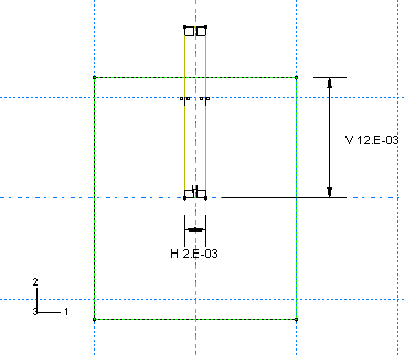
Sketch the profile of the cut shown in
Figure 1.
Use a Symmetry constraint to center the cut about the
construction line and edit the dimensions of the cut profile so that it is
0.002 m wide and extends a distance of 0.012 m into the packaging.
Figure 1. Profile of cut in packaging (with grid spacing doubled).

- In the Edit Cut Extrusion dialog box that appears upon completion of the sketch, select Through All as the end condition and select the arrow direction representing a cut into the packaging.
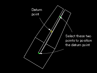
Create a datum point centered on the bottom face of the cut, as shown in Figure 2. This point will be used to position the board relative to the packaging.
Figure 2. Datum point at center of cut in packaging.
-
From the main menu bar, select
ToolsDatum.
The Create Datum dialog box appears.
- Accept the default selection of Point as the datum type and select Midway between 2 points as the method.
-
Select the two points centered on the bottom face at either end of
the cut to be the two points between which the datum point will be created.
Abaqus/CAE creates the datum point shown in Figure 2.
-
From the main menu bar, select
ToolsDatum.
![]()
Define the circuit board geometry
The circuit board can be modeled as a thin, flat plate with chips attached to it. Create a three-dimensional, deformable planar shell to represent the circuit board; name the part Board. Use an approximate part size of 0.5, and sketch a 0.100 m × 0.150 m rectangle for the profile.
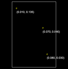
Create the three datum points shown in Figure 3. These points will be used to position the chips on the board.
Figure 3. Datum points used to position the chips relative to the board. Numbers in parentheses are (x, y) coordinates in meters based on a local origin at the bottom left corner of the circuit board.
-
From the main menu bar, select
ToolsDatum.
The Create Datum dialog box appears.
- Accept the default selection of Point as the datum type, and select Offset from point as the method.
- Select the bottom left corner of the board as the point from which to offset, and enter the coordinates for one of the points shown in Figure 3.
- Repeat Step c to create the other two datum points.
-
From the main menu bar, select
ToolsDatum.
![]()
Define the floor
The surface that the circuit board will impact is effectively rigid. Create a three-dimensional, discrete rigid planar shell to represent the floor; name the part Floor. Use an approximate part size of 0.5. The rigid surface should be large enough to keep any deformable bodies from falling off the edges.
Sketch a 0.2 m × 0.2 m square as the profile. To simplify the positioning of parts in the assembly of the model, ensure that the center of the surface corresponds to point (0, 0) in the sketcher. This also corresponds to the origin of the global coordinate system.
Assign a reference point at the center of the part.